- 面议
起订量:
Telluride 碲化物
- 型号
- 参数
- 供货周期:一周

该企业相似产品


上海巨纳科技有限公司是巨纳集团旗下科学仪器事业部。巨纳集团SUNANO GROUP产业格局包括新能源业务、通信业务、现代贸易业务、微纳米业务、科研检测业务、投资管理业务等。旗下上海巨纳科技有限公司是集多种高科技产品的研发、生产、销售为一体的企业,同时是多家世界高科技公司在中国的总代理。2015年起正式并入巨纳集团科学仪器事业部体系并作为其大陆运营主体。
巨纳集团科学仪器事业部,主要致力于研究开发和整合仪器设备,从事表面科学、分析仪器、生命科学设备、光伏设备及实验室仪器的设计、开发和制造及分销;为科研、教育、检测及生产提供完整可靠的解决方案,已经成为了众多高校和企业的优质供应商。
近年来巨纳集团科学仪器事业部先后收购了高纯水机、光学平台、真空干燥箱等制造企业,创立了SUNANO、NextCVD、低维材料在线91cailiao、FIPHENE、GRCC等品牌,并与韩国Nanoscope System、日本HORIBA、英国Oxford Instruments、美国CRAIC、法国PhaseView、瑞士LynceeTec等品牌深入合作,加强了公司产品的多样化。
巨纳集团科学仪器事业部为您的研究与分析提供先进工具与解决方案:
光学光谱·分子光谱·元素分析·表面测量·颗粒表征·光学平台·激光共聚焦显微镜·激光荧光共聚焦显微镜·共焦激光拉曼光谱仪·便捷式激光拉曼光谱仪·椭圆偏振光谱仪·激光粒度仪·多功能宽密度等离子体ICP-LP-PE-CVD·碳/硫分析·氧/氮/氢分析·等离子体发射光谱仪·辉光放电光谱仪··全息数字显微镜··高纯水机··各类干燥箱/培养箱/离心机/搅拌器/高速分散器/水浴锅/振荡器/低温槽/加热槽·低维材料等。
韩国Nanoscope Systems是激光共聚焦显微镜开发商和制造商,拥有微纳米尺度上的光学表面测量技术,主要产品激光共聚焦显微镜和激光荧光共聚焦显微镜广泛用于工业领域和科学研究中的三维测量和检查,为三星、LG、SK海力士、韩华集团、V-technology等世界企业提供精密的解决方案。作为共聚焦显微技术的开发者和提供者,韩国Nanoscope System致力于以更高的分辨率、更高速度的三维测量的新技术。 除了半导体、FPD、MEMS、OLED、太阳能、材料等领域,加上荧光和热反射功能,在生物、化学和医疗领域也有出色的应用。巨纳作为韩国Nanoscope System在中国区域的总代理,全面负责经营销售及售后服务等业务。
详细信息
Our R&D team are about to release new Tellurene nanowires series (in late March,2018), you may pre-order these products when order regular Tellurene single crystals.
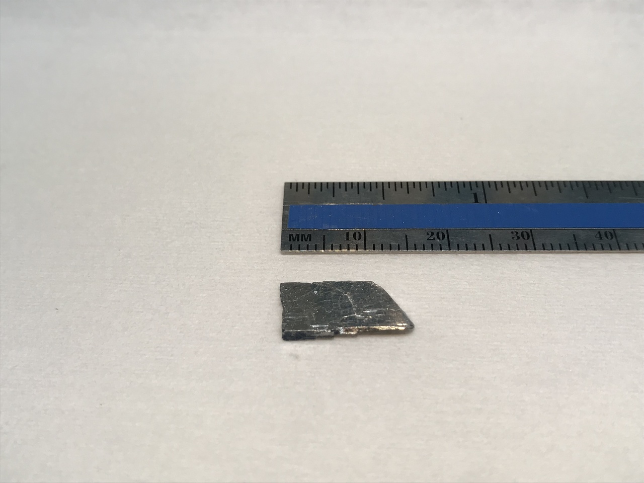
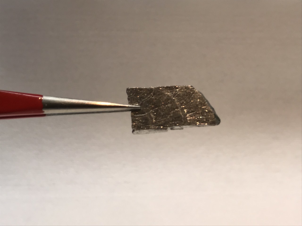
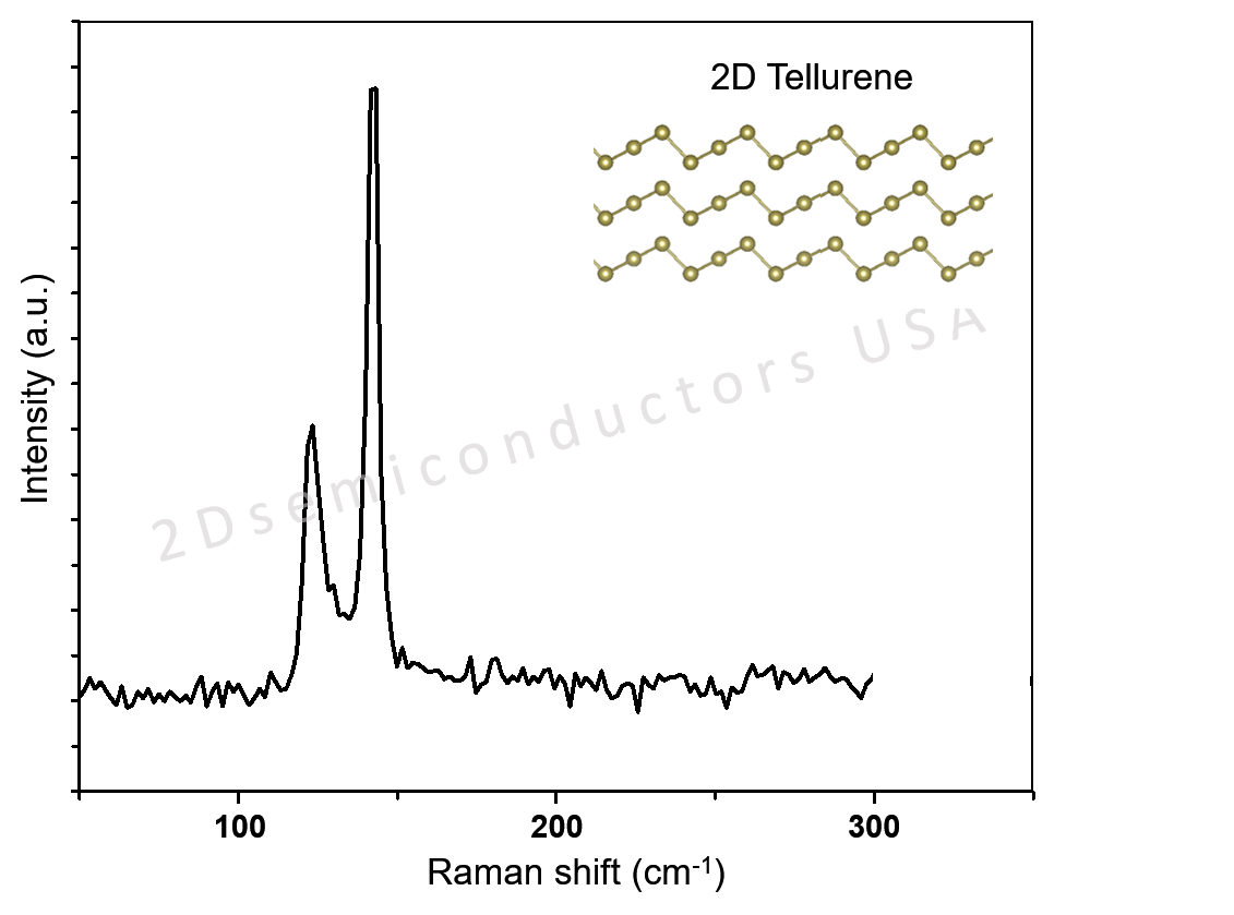
The first commercial vdW Tellurium (b-phase) crystals. Layered tellurium crystals have been synthesized in perfectly vdW order through flux zone growth technique. The crystal has 99.9999% (6N) rated purity and has been crystalized in perfect atomic order.
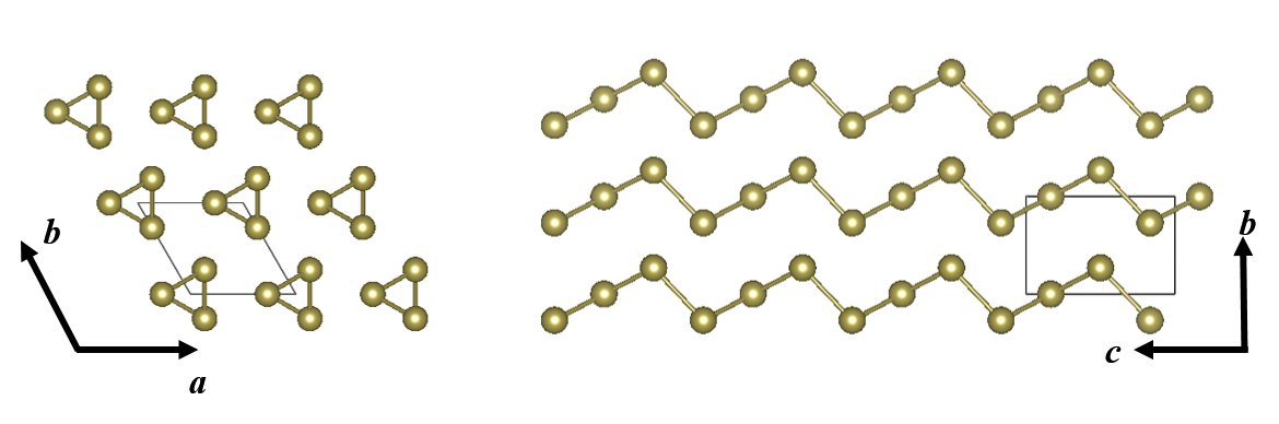
Layered tellurium (Te) has a trigonal crystal lattice (see product images) in which individual helical chains of Te atoms are stacked together by van der Waals type bonds and spiral around axes parallel to the [0001] direction at the center and corners of the hexagonal elementary cell [1-2]. Tellurene exhibits a tunable bandgap varying from nearly direct 0.31 eV (bulk) to indirect 1.17 eV (2L) and direct at 1.3 eV (1L) [3]. It has four (two) complex, highly anisotropic and layer-dependent hole (electron) pockets in the first Brillouin zone with an extraordinarily high hole mobility reaching up to theoretical ∼1E5 cm2/Vs value [1-3].
Material characteristics
High carrier mobility semiconductor
Tunable IR semiconductor (Eg ranging from 0.3 to 1.3 eV from bulk to monolayers)
2D anisotropic semiconductor
Physical size ~1cm or larger;
Note: This product is same as tellurene material. While material itself is perfectly crystallized in trigonal form (weakly coupled Te chains are present), it is inherently harder to exfoliate in comparison to graphene or MoS2. For best results, we recommend using strongly adhesive tapes or liquid exfoliation technique.
Related references
[1] "Two-dimensional tellurium" Nature 552, 40-41 (2017)
[2] "Large-area solution-grown 2D tellurene for air-stable, high-performance field-effect transistors"; arXiv:1704.06202
[3] "Few-layer Tellurium: one-dimensional-like layered elementary semiconductor with striking physical properties" ; https://doi.org/10.1016/j.scib.2018.01.010