其他品牌 品牌
生产厂家厂商性质
上海市所在地
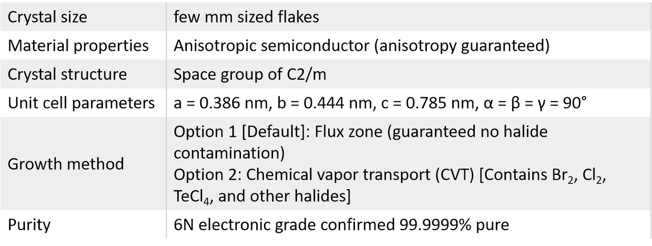
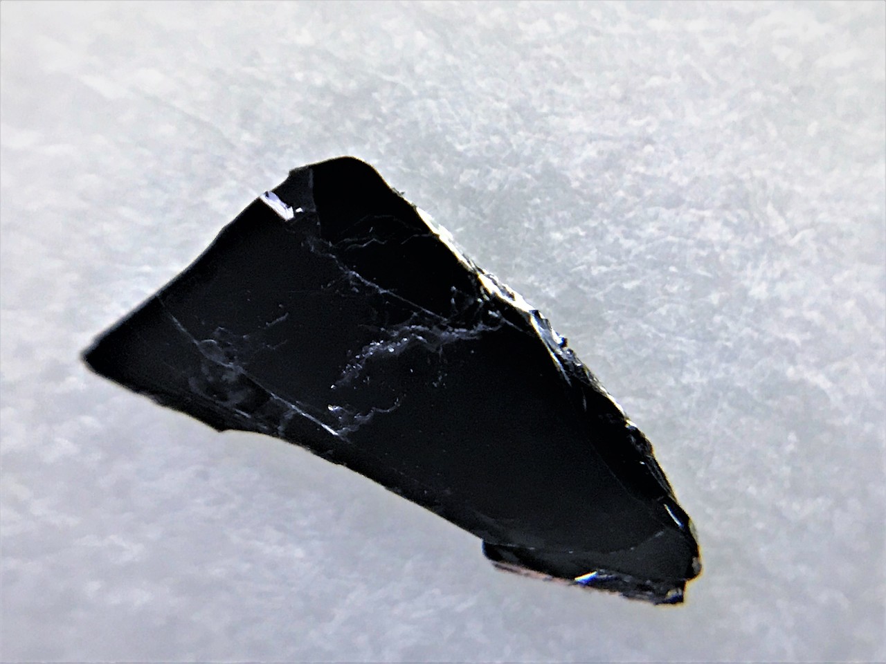
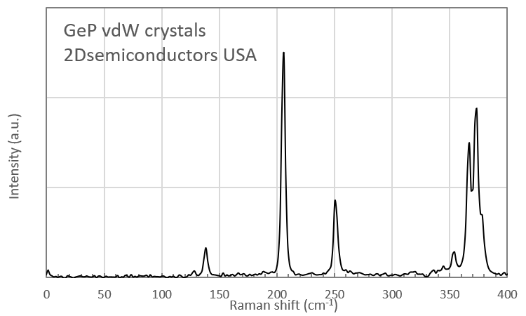
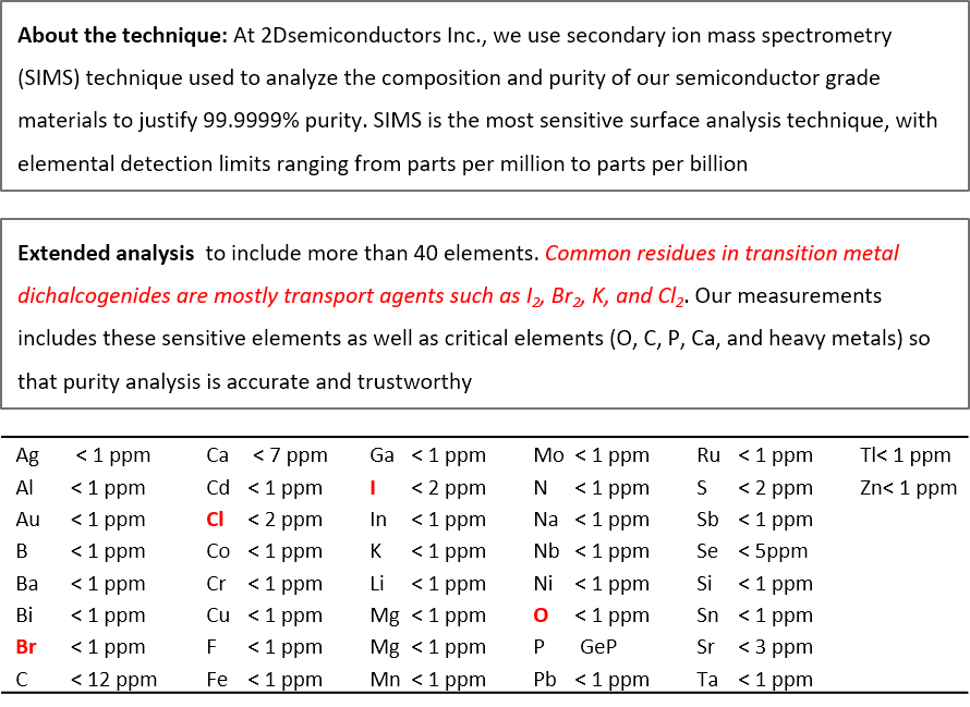
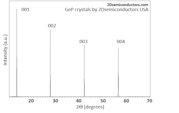
GeP has highly anisotropic dispersions of band structures, with a layer-dependent indirect band gap from (theoretically predicted) 1.68 eV of monolayer to 0.51 eV of bulk. GeP is an anisotropic semiconductor much similar to GaTe monoclinic structure. Our single crystal GeP (Germanium phosphide) crystals come with guaranteed optical, electronic, and structural anisotropy. They are developed at our facilities using state-of-art flux zone techniques. Each growth takes close to three months to provide you perfected crystals that does not contain any halides. Each crystal is highly crystalline, oriented in 0001 direction, and easy to exfoliate. Our R&D staff takes characterization dataset in each sample piece to ensure structural, optical, and electronic consistency. Please also see our GeS, GeSe, GeTe, GeAs, GeP, and Ge-based solutions.
Characteristics of vdW GeP crystals