What is Nano SOI?
Rapid fabrication service for prototyping silicon photonic integrated circuits. Includes passive and thermo-optic devices.
Turnaround time from design submission to delivery as short as three weeks.
Options for cladding oxide, metallization, and deep trenches for edge-coupling.
Proven optical performance and low propagation loss.
Introduction
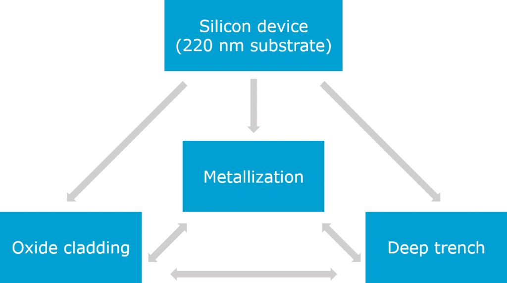
The NanoSOI fabrication process provides an avenue to fabricate photonic integrated circuits (PICs). The foundation of the process is the silicon patterning step, which is performed on silicon-on-insulator (SOI) substrates. Superior line-edge roughness and high throughput are guaranteed with the use of a state-of-the-art 100 keV electron-beam lithography system. Our anisotropic plasma etch process provides smooth sidewalls for reduced scattering loss in photonic devices. Optional process steps such as oxide cladding deposition, metallization and deep trench etching can be performed afterward to create passive and active photonic devices with grating couplers or edge couplers. In addition to these standard processes, we also have custom options available such as selective oxide removal, or partial etch depths.
 There are two options for accessing the NanoSOI fabrication process. Multi-project wafer (MPW) runs are scheduled once every two months. Standard processes and immediate pricing are available for these runs. Dedicated runs are for projects requiring custom options such as selective oxide release. Timelines for these runs are flexible, and quotations are customized for each run.
Submission Process
Submission of a design to the NanoSOI process is done online. Design files are provided to us in Calma Graphics Data System II (GDSII) format, with database units of 1 nanometre. Designs are submitted online using the NanoSOI Design Center, which can be accessed by choosing “Submit A Design” in the navigation bar above. The latest design rules, layout tutorials, and details about the fabrication process are all located at the NanoSOI Design Center. Pricing for multi-project wafer runs is also available online through the Design Center.
Fabrication Details
Our fabrication process, including all of our standard options, is outlined below. Jump to any process step using the sidebar on the right.
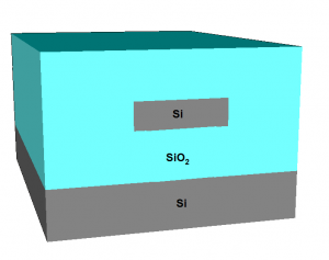
Silicon Device Layer
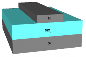 Our silicon patterning process involves the definition of nano-scale features in silicon-on-insulator (SOI) using electron beam lithography (EBL) and reactive ion etching (RIE) processes. The substrate is a 220 nm silicon device layer with a 2 µm buried oxide layer and 675 µm handle wafer. The patterning process begins by cleaning and spin-coating a material that is sensitive to electron beam exposure. A device pattern is defined into this material using 100 keV EBL. Once the material has been chemically developed, an anisotropic ICP-RIE etching process is performed on the substrate to transfer the pattern into the underlying silicon layer. The etch is performed until there is no remaining silicon and the underlying buffer oxide layer is exposed. Once the silicon patterning step has been completed, several standard options become available to add extra functionality to the device, including oxide deposition to protect and isolate silicon devices, metallization to give the devices electrical functionality, and deep trenches to provide a smooth interface for fiber edge-coupling. Custom options include selective oxide release to create free-standing silicon structures for mechanical applications.
Waveguide Components
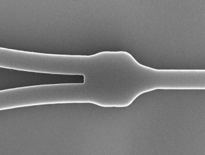
Y Splitter (50/50) on 220 nm SOI
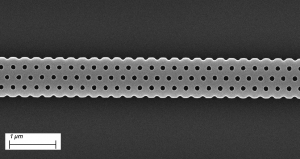
Grating Couplers
Sub-wavelength grating coupler patterned on 300 nm SOI
Photonics Crystals
Photonic crystal strip waveguide patterned on 300 nm SOI
Propagation Loss measurements
Applied Nanotools periodically measures the optical propagation loss using test structures. The test structure is a straight 500 nm-wide silicon strip waveguide with a 2.2 μm-thick cladding oxide. Cut-back loss measurements are performed by varying the length of the waveguide from 0 to 3 centimetres, measuring the total insertion loss of each device and performing a linear fit on loss vs. waveguide length. Both straight and curved waveguide segments are used. The average propagation loss for fully-etched 220 nm SOI devices is tabulated below:
| Polarization | Straight Waveguide Loss | Curved Waveguide Loss |
|---|
| TE | 1.5 dB/cm | 3.8 dB/cm |
| TM | 2.4 dB/cm | 3.0 dB/cm |
These results are averaged over two sets of test arrays. Each set was separated by 9 mm. Detailed measurement data, including spectral scans, can be provided by request.
Oxide Deposition
 If the silicon devices require isolation from the outside environment, silicon dioxide can be deposited onto the device using a chemical vapour deposition (CVD) process. Our standard oxide deposition thickness is is 2.2 µm, which is sufficient for most thermal and optical applications. The oxide deposition process can be combined with our tri-layer heater metallization process to fabricate active photonic devices that can be controlled with temperature. Custom oxide thicknesses up to 3 µm can be requested.
Metalization
Metallization adds electrical functionality to your device. ANT has two metallization processes, which are either performed directly on the silicon features or on top of the oxide cladding (if deposited in the previous step). The former enables the direct application of a voltage/current to a silicon device, and the latter enables low-loss thermo-optic photonic devices.
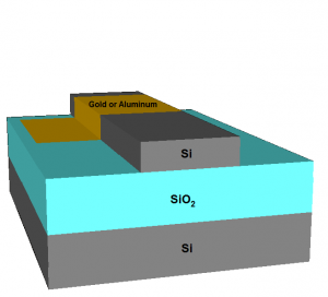
Derect Metalization
the purpose of direct metallization is to create bonding and/or probing pads and to pattern coarse electronic pathways directly on the silicon devices. This metallization process uses photolithography to define the metal areas (minimum 10 µm feature size) to within a 2 µm alignment precision to the underlying silicon layer. Metals are deposited on the substrate using electron-beam evaporation and the thickness can be controlled to an accuracy of ±5 % of the overall thickness. Oxide cladding cannot be deposited on the device before direct metallization is performed. The standard metal is Au. Aluminum or other custom metals can be used upon request. The choice of materials for the pads/traces are as follows:
| Metal | Thinkness |
|---|
| Gold (with 4 nm Cr adhesion layer) | 100 nm |
Tri-layer metalization
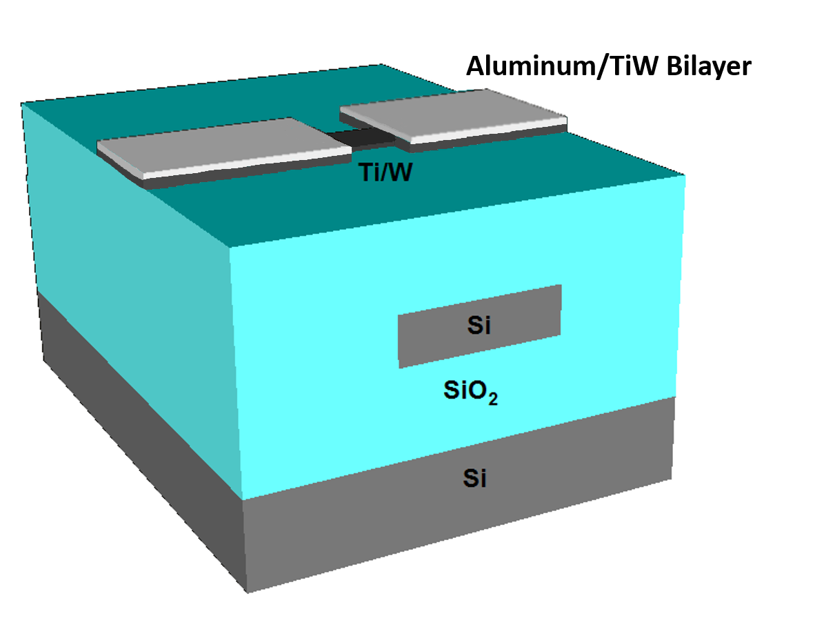
* Protective oxide layer not shown.
The purpose of tri-layer metallization is to create compact heater devices using a high-resistance metal and interface with the heater devices using a low-resistance routing layer. A third layer consisting of silicon dioxide is used to protect the heaters from oxidation damage. The oxide is etched away over the aluminum pads to expose them for probing or wire bonding. The use of two metals increases the electrical efficiency of the devices, as the majority of the heat generation can be targeted to a specific area of the chip with the Ti/W. The two metal layers are also patterned using photolithography. The heater layer uses a titanium-tungsten alloy to implement the high-resistance heater devices. The routing layer, which can consist of wider electrical traces or bonding/probing pads, is made out of a titanium-tungsten/aluminum bilayer. Using a bilayer for the routing layer ensures good electrical contact between the routing layer and the heater layer with low contact resistance. The bilayer also ensures that the routing layer is uniform layer with no height changes. A blanket layer of oxide is then deposited on the chips and the probing pads are exposed using the oxide window layer. Below are the specifications of the tri-layer
| Metal | Thinkness |
|---|
| TiW Alloy Heater Layer | Thickness: 200 nm Bulk Resistivity: 0.61 μΩ-m Sheet Resistance: 3.07 Ω/sq |
| TTiW/Al Bilayer Routing Layer | Thickness: 200 nm Ti/W + 500 nm Al Bulk Resistivity: 0.04 μΩ-m Sheet Resistance: 0.08 Ω/sq |
| Silicon Dioxide Protective Layer | Thickness: 300 nm Bulk Resistivity: N/A Sheet Resistance: N/A |
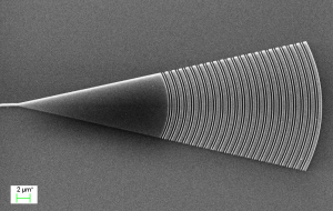
Deep Trench Etch
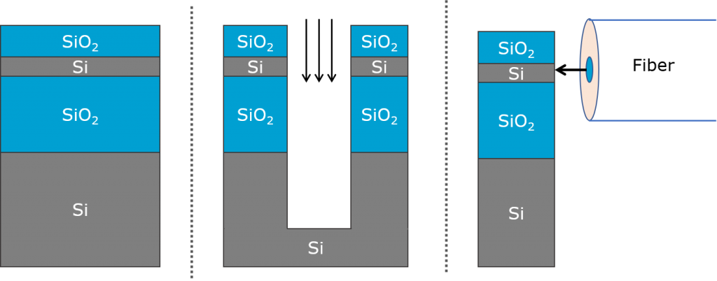
With our deep-etch process, trenches can be made along the perimeter of the chip to allow for a fiber optic cable to couple light directly into on-chip devices such as nano-tapered waveguides and sub-wavelength gratings. The 300 μm-wide trench is patterned around an 8.78 x 8.78 mm enclosed area, centered on the submitted GDSII design. A deep-etch process is then used to etch through the cladding, buried oxide, and through the underlying silicon substrate. The final result is a 8.78 x 8.78 mm substrate with a smooth interface on all four sides for fiber edge-coupling.