
Osslia 品牌
代理商厂商性质
长沙市所在地

1-materia材料PTB7 CAS#1237479-39-8 OS0007
面议
Gibco胎牛血清16000-044 进口胎牛血清 Gibco血清
面议
澳洲胎牛血清10099-141 Gibco胎牛血清10099141 进口胎牛血清
面议1-material材料PSBTBT-n 1160106-18-2
面议
1-Material PDPP2T-TT-OD OS0749化学试剂
面议
加拿大1-Material材料PCE-10
面议
Allgaier器械
面议
EXCELTA代理
面议Biovision试剂盒K254-200 ApoSENSOR ATP细胞活力分析试剂盒
面议Excelta
面议
Kent小鼠气管插管器械包
面议
大鼠解剖器械包 Kent动物解剖
面议只用于动物实验研究等
PTB7 for high-performance organic photovoltaics.
Poly[[4,8-bis[(2-ethylhexyl)oxy]benzo[1,2-b:4,5-b']dithiophene-2,6-diyl][3-fluoro-2-[(2-ethylhexyl)carbonyl]thieno[3,4-b]thiophenediyl]], more commonly known as PTB7.
In stock now for immediate dispatch worldwide.
PTB7 gives some of the highest reported efficiencies for polymer:fullerene solar cells due to its extended absorption into the near infra-red and lower HOMO level. Together with our complete package of processing information, PTB7 becomes a quick and easy way to improve device efficiencies. This represents a cost-effective method to increase performance and impact of devices and data for a wide range of OPV related research.
At typical concentrations for spin-coated devices of 10 mg/ml, a standard batch of 100 mg will produce 10 ml of ink - enough to coat 200 of Ossila's standard sized substrates even assuming 50% ink loss during preparation and filtration. At concentrations of 1 mg/ml (more typical for ink-jet printing and spray coating) up to 100 ml of ink can be produced.
In a standardised reference architecture (using a PEDOT:PSS hole interface and Ca/Al electron interface) we have shown this batch to give a PCE of 6.8% (see data sheet below) and up to 7.4% using PFN. By using new interface materials and architectures PTB7 has been shown to reach efficiencies of 9.2% PCE in the literature [1,2].
The high solubility in a wide range of solvents makes ink preparation and filtration simple, and PTB7 is one of the easiest materials we have ever worked with (simply shake it to dissolve). This also makes it an excellent candidate for a variety of coating techniques including ink-jet printing, spray coating and blade coating.
For information on processing please see our specific fabrication details for PTB7, general fabrication video,general fabrication guide, optical modelling paper on our standard architecture [3], or us for any additional help and support.
References (please note that Ossila has no formal connection to any of the authors or institutions in these references):
Ossila材料PTB7 CAS:1266549-31-8 Ossila材料M213
<:figure style="BOX-SIZING: border-box; TEXT-ALIGN: center; WIDOWS: 1; TEXT-TRANSFORM: none; BACKGROUND-COLOR: rgb(255,255,255); TEXT-INDENT: 0px; MARGIN: 0px; DISPLAY: block; FONT: 14px/20px 'Open Sans', 'Open Sans', 'Liberation Sans', 'Helvetica Neue', Helvetica, sans-serif; WHITE-SPACE: normal; LETTER-SPACING: normal; COLOR: rgb(51,51,51); WORD-SPACING: 0px; -webkit-text-stroke-width: 0px">
Chemical structure of PTB7; Chemical formula (C41H53FO4S4)n.
| Full name | Poly[[4,8-bis[(2-ethylhexyl)oxy]benzo[1,2-b:4,5-b']dithiophene-2,6-diyl][3-fluoro-2-[(2-ethylhexyl)carbonyl]thieno[3,4-b]thiophenediyl]] |
| Synonyms | PTB7 |
| CAS number | 1266549-31-8 |
| Absorption | 670 nm (CH2Cl2), 682 nm (film) |
| Solubility | Chloroform, Chlorobenzene, o-DCB |
Ossila材料PTB7 CAS:1266549-31-8 Ossila材料M213
Reference device were made on batch M211 to assess the effect of PTB7:PC70BM active layer thickness on OPV efficiency using an inverted architecture with the below structure. These consisted of the below structure and were fabricated under inert atmosphere (glovebox) before encapsulation and measurement under ambient conditions.
Glass / ITO (100 nm) / PFN (6.5 nm) / PTB7:PC70BM (1:1.5) / MoOx (15 nm) / Al (100 nm)
For generic details please see the general fabrication guide and video. For specific details please see the below condensed fabrication report which details the optical modelling and optimisation of the multilayer stack.
Previously it has been shown that PFN of around 6.5 nm gives optimum performance [1-3,P021] while modelling has shown that an Al back cathode gives higher performance than Ag when used with MoOx [4].
The PTB7:PC70BM solution was made in chlorobenzene at 25 mg/ml before being diluted with 3% diiodooctane (DIO) to promote the correct morphology.
Active layer thicknesses of 75 nm, 90 nm and 105 nm were chosen corresponding to the lower, middle and upper end of the "thin film" absorption peak of a typical stack as predicted by optical modelling [1]. For each of these thickness a total of four substrates was produced, each with 4 pixels and the data presented below represents a non-subjective (no human intervention) analysis of the best 75% of pixels by PCE (12 pixels for each condition).
An additional two substrates were also prepared with a methanol wash to help remove the DIO as has been reported in the literature to help improve performance[5].
Overall, the maximum efficiency of 7.2% average PCE (7.4% maximum) was found at 75 nm film thickness.
Note 1: Dektak Thickness calibration
We normally calibrate thin films by use of a Dektak surface profiler, however the use of DIO results in an enhanced level of uncertainty in the film as the DIO will take several hours to fully dry under normal conditions and is likely to undergo some slight further shrinkage when placed in vacuum. The DIO can also be removed by baking the substrate on the hotplate at 80°C for about 10 mins which can be useful for doing quick measurements but also drives excess phase separation between the polymer and PCBM making it unsuitable for device work.
Note 2: Effect of epoxy
Due to the very high solubility of the PTB7 it was noted during fabrication that the film changed colour when in contact with the EE1 encapsulation epoxy in liquid form for extended periods indicating that there was some miscibility. Inspection of the active areas underneath the top cathode indicated that the epoxy had not seeped into the active area before curing and device metrics indicate that this did not appear to affect performance. However, we would recommend minimising contact time between the epoxy and PTB7 films before UV curing.
Fabrication
Substrates and cleaning
PFN Solution
PFN Test Films
Active Layer Solution
Active Layer Test Films
Active layers
Evaporation
Left in chamber over the weekend and evaporated with the below parameters.
Encapsulation
Measurements
Reference device were made on batch M211 using a standardised architecture for comparative measurements using Ossila standard substrates and materials. These consisted of the below structure and were fabricated under inert atmosphere (glovebox) before encapsulation and measurement under ambient conditions.
Glass / ITO (100 nm) / PEDOT:PSS (30 nm) / PTB7:PC70BM (variable) / Ca (2.5 nm) / Al (100 nm)
For generic details please see the fabrication guide and video. For specific details please see the below condensed fabrication report and also Watters et al. [3] which details the optical modelling and optimisation of the multilayer stack.
For this standard reference architecture an average PCE of 6.6% was achieved for the optimised thickness with a peak efficiency of 6.8%. Note that no other optimisation was performed (blend ratio, DIO concentration, drying conditions etc) and so further small improvements may be obtained by varying these conditions and significant improvements obtained by using alternative interface materials [1,2].

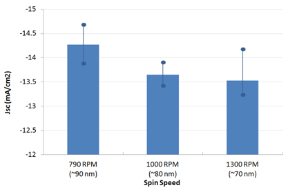
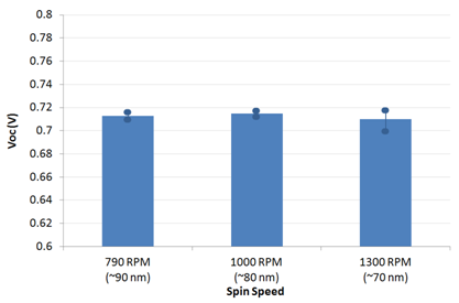
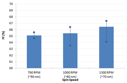 Figure 3: PCE, Jsc, Voc and FF for standard architecture devices at different spin speeds. Data shown is averaged with max and min overlaid with filled circles (please see note of Dektak measurements). As previously reported [1,2,3], films of approximay 90 nm give the highest performance with greater Jsc and only minor loss in fill factor.
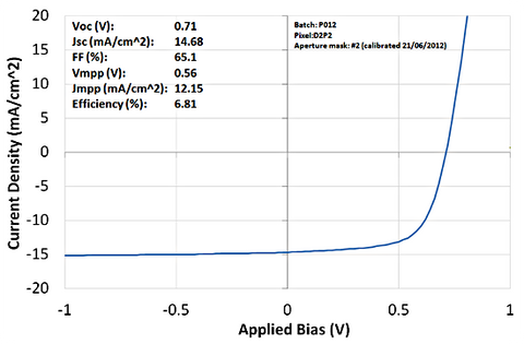
Figure 4: The JV curve for the best performing device - standard architecture.
Note 1: Dektak Thickness calibration
We normally calibrate thin films by use of a Dektak surface profiler, however the use of DIO results in an enhanced level of uncertainty in the film as the DIO will take several hours to fully dry under normal conditions and is likely to undergo some slight further shrinkage when placed in vacuum. The DIO can also be removed by baking the substrate on the hotplate at 80°C for about 10 mins which can be useful for doing quick measurements but also drives excess phase separation between the polymer and PCBM making it unsuitable for device work.
Note 2: Effect of epoxy
Due to the very high solubility of the PTB7 it was noted during fabrication that the film changed colour when in contact with the EE1 encapsulation epoxy in liquid form for extended periods indicating that there was some miscibility. Inspection of the active areas underneath the top cathode indicated that the epoxy had not seeped into the active area before curing and device metrics indicate that this did not appear to affect performance. However, we would recommend minimising contact time between the epoxy and PTB7 films before UV curing.
Fabrication
Substrates and cleaning
PEDOT:PSS layer preparation
Active layer Solution Preparation
Active layer spin casting
Evaporation
Left in chamber over the weekend and evaporated with the below parameters.
| Material | Ca |
| Base pressure | 8.0 E-8 mbar |
| Dep start pressure | 1.7 E-7 mbar |
| Max pressure | 2.7 E-7 mbar |
| Thickness | 2.5 nm |
| Rate | 0.2 Å/s |
| Material | Al |
| Base pressure | 7.0 E-8 mbar |
| Dep start pressure | 6.0 E-7 mbar |
| Max pressure | 7.0 E-7 mbar |
| Thickness | 100 nm |
| Rate | 1.0 Å/s |
Encapsulation
Measurements
To the best of our knowledge the technical information provided here is accurate. However, Ossila assume no liability for the accuracy of this information. The values provided here are typical at the time of manufacture and may vary over time and from batch to batch.


